Learning and Education
EMI/EMC Courses

Secrets of EMI/EMC Design and Troubleshooting with Near-Field Scanning
An excellent one-day course for designers and manufacturers of electronic products
Enjoy a really practical and useful course discovering the fundamentals of practical EMI/EMC design and troubleshooting of electronic circuits. Discover the really powerful design and troubleshooting, techniques and tools to “see” and “feel” your problems. The fundamentals of EMI/EMC problems are explained in a very easy and practical way.
Overview:
- EMI/EMC fundamentals
- EMI sources/victims
- Radiated and conducted emission/immunity
- Control of current path: DM vs CM
- Voltage and current measurements
- Electric and magnetic measurements
- Technics to find culprits and victims
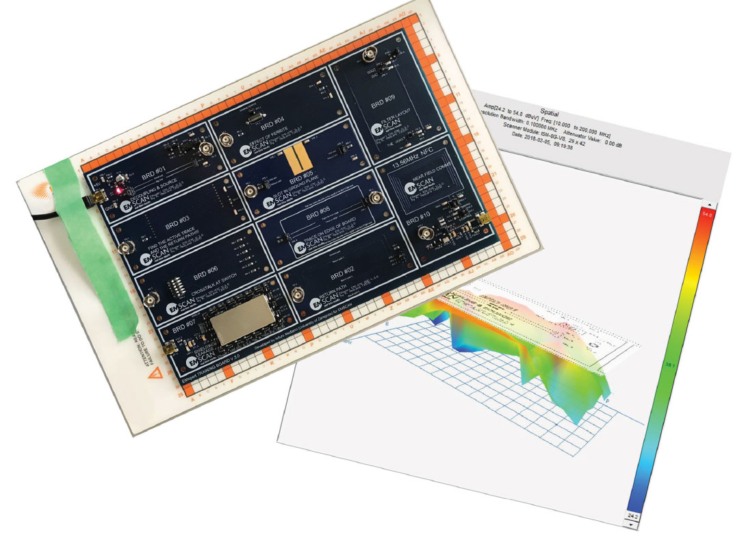
- Analysis and troubleshooting with a near-field scanner
- Spectral scan and spatial scan
- Examples and demos
INSTRUCTOR
Prof. Arturo Mediano
University of Zaragoza
Book your place today
SCANNER USERS

Testimonials
The instrument provides spatial and spectral scans that allow design teams to cut one to two design cycles out of their product development process. It also reduces their EMI testing time by up to two orders of magnitude.
The design team conducted the scans on the EMxpert system in their offices. In a matter of minutes, they obtained the results. Testing the design in a third party chamber would have have been weeks away